Research in Detail

Oxide Electronics
Investigating fundamental electronic transport and device physics in crystalline and amorphous oxide semiconductors.
We investigate electronic transport in crystalline and amorphous oxide semiconductors, such as WO3, W-doped InO, etc. We utilize various methods such as Hall measurements, cryogenic measurements, and low-temperature characterization, combining these with numerical and analytical modeling to characterize and understand fundamental electronic transport mechanisms.
Additionally, we develop thin film transistors (TFTs) using these materials for various applications.
Key focus area:
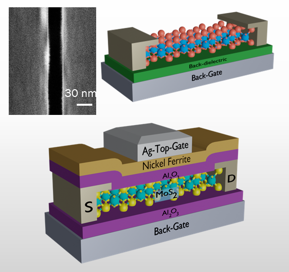
2-D Logic FETs
Engineering highly scaled nodes and energy-efficient logic through atomically thin semiconductors.
Technology scaling has driven the development of semiconductor technology. However, efforts to continue scaling have met numerous challenges, both from engineering limitations and the fundamental limits of silicon. Two-dimensional (2-D) materials are a potential candidate for highly scaled nodes due to their atomically thin nature and excellent electrostatics.
My research in 2D electronics encompasses various aspects, including contact and gate stack engineering, steep subthreshold slopes FETs, and ultra-scaled short-channel FETs.
Outcome
- Publication: Sub-1V Threshold switching in Microwave Assisted Solvothermal Nickel Ferrite Films and its application for steep switching MoS₂ phase FETs (ACS AMI 2024)
- Publication: Alcohol-Based Sulfur Treatment for Improved Performance and Yield in MoS₂ FETs (IEEE TED 2020)
- Publication: Performance tunability of field-effect transistors using MoS₂ Se alloys (Nanotechnology 2021)
- Publication: Hafnia-based Phase-Change Ferroelectric Steep-Switching FETs on a 2-D MoS₂ platform (Under Review)
- Conference: Enabling Al₂O₃ top gate dielectrics on MoS₂ - mitigating the doping problem (Poster, Graphene Week 2023)
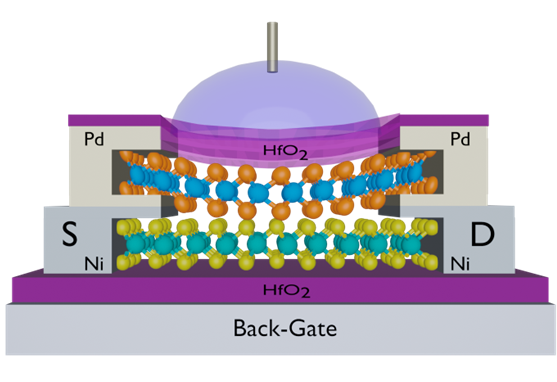
ISFETs for Sensing
Developing CMOS-compatible bio-FETs for high-precision chemical and bio-sensing.
Two-dimensional (2-D) materials show promise for highly scaled nodes because of their atomically thin composition and exceptional electrostatic properties. The remarkable surface-to-volume ratio and sensitivity to external factors also make 2-D materials ideal for bio-sensing applications. By appropriately functionalizing field-effect transistor (FET) technology, ion-sensitive FETs (ISFETs) can be created for detection of pH and various biomolecules.
Despite the advantages of CMOS platforms, ISFETs suffer from major bottlenecks, which includes limited sensitivity (< 59 mV/pH, the Nernst limit), need for isolation, and challenges in reliability due to problems like drift. In our lab, we investigate device architectures and innovations to surpass these challenges. The Nernst limit must be surpassed to achieve higher resolution measurements of pH and biomolecules. Through a heterostructure of WSe2 and MoS2, we have demonstrated super-Nernstian pH sensitivity, reaching 346 mV/pH. This device capitalizes on the charge screening effect of the interface and inversion charges at the heterointerface for enhanced sensitivity. Additionally, we've utilized a TCAD-based approach, integrating ferroelectric negative capacitance effect onto the WSe2/MoS2 heterostructure device, and demonstrated sensitivities reaching 4.38 V/pH.
Key focus area:
Outcome
- Publication: Super-Nernstian ion sensitive field-effect transistor exploiting charge screening in WSe₂/MoS₂ heterostructure (npj 2D Mater Appl 2021)
- Publication: Super-Nernstian WSe₂/MoS₂ heterostructure ISFET combining Negative Capacitance and Charge Screening Effects (IEEE Sensors J 2023)
- Publication: Monolithic pH Sensing via Frequency Modulation in 2D NC-ISFET-Based Ring Oscillators (IEEE Sensors J)
- Publication: Enzyme functionalized MoS₂ bio-FETs for ultra-sensitive detection of cholesterol (Under preparation)
- Book Chapter: Functionalized Nanomaterials for Designing Nano/Micro Biologically Sensitive Field-Effect Transistors (Bio-FETs) (Wiley 2025)
- Conference: Super-Nernstian ISFET Combining Two-Dimensional WSe₂/MoS₂ Heterostructure with Negative Capacitance (Digital Invited Talk, 242nd ECS Meeting 2022)
- Conference: Super-Nernstian ISFET Using Scaled Coplanar Multi-Gated Channels (Oral, IEEE Sensors 2023)
- Conference: Super-Nernstian Floating-Extended Gate Ion Sensitive Field Effect Transistor for pH sensing (Poster, IEEE Sensors 2023)
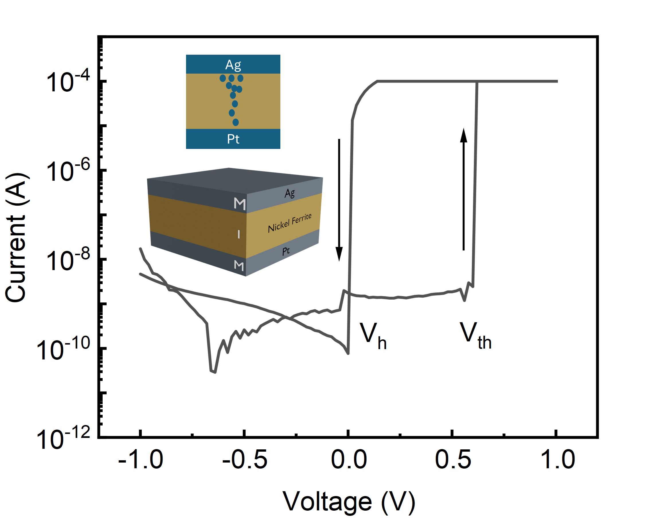
Beyond Moore Devices
Memristive devices, neuromorphic computing, ferroelectric FETs, and more.
My "Beyond Moore" research explores novel physical effects to overcome the fundamental limits of classical computing. This includes exploring filamentary devices showing memristive and threshold switching activity. I also explore switching activity in various material systems including gate stack engineered MoS2-HfO2 and hBN systems.
I use high-speed electrical measurements to study these emerging devices with eventual applications targeting both conventional and emerging Neuromorphic computing platforms.
Outcome
- Publication: Realizing avalanche criticality in neuromorphic networks on a 2D hBN platform (Materials Horizons 2023)
- Publication: Artificial Synapse Based on Back‐Gated MoS2 Field‐Effect Transistor with High‐k Ta2O5 Dielectrics (physica status solidi (a) 2020)
- Publication: Sub-1 V Threshold Switching in Microwave-Assisted Solvothermal Nickel Ferrite Films and Its Application for Steep Switching MoS2-Phase FETs (ACS AMI 2024)
- Conference: Brain-like avalanche behavior in filamentary networks of memristive Ag-hBN system (Proc. of Materials, Devices and Systems for Neuromorphic Computing)
TCAD Simulation & Modelling
Leveraging advanced simulation tools (Silvaco, Sentaurus, Ginestra) for predictive modelling, device optimization, and inference of device physics.
TCAD simulation is used whenever necessary, providing deep insights into device physics that are often inaccessible through experimental characterization alone. I utilize industry-standard tools like Silvaco ATLAS, Sentaurus TCAD, and Ginestra to model FETs, ISFETs, gate stacks, and complex heterostructures.
Non-standard functions can be realized by integrating user-defined material models for 2-D materials, emulating electrolyte interactions, and combining with numerical models in Matlab/Python. This helps in predicting device behavior, understanding physical mechanisms, and optimizing device architecture. This synergy between simulation and experimental nanofabrication significantly accelerates the development cycle for next-generation nano-electronic devices.
Outcome
- Publication: Super-Nernstian ion sensitive field-effect transistor exploiting charge screening in WSe₂/MoS₂ heterostructure (npj 2D Mater Appl 2021)
- Publication: Super-Nernstian WSe₂/MoS₂ heterostructure ISFET combining Negative Capacitance and Charge Screening Effects (IEEE Sensors J 2023)
- Publication: Monolithic pH Sensing via Frequency Modulation in 2D NC-ISFET-Based Ring Oscillators (IEEE Sensors J)
- Conference: Super-Nernstian ISFET Combining Two-Dimensional WSe₂/MoS₂ Heterostructure with Negative Capacitance (Digital Invited Talk, 242nd ECS Meeting 2022)