Nanoelectronics

Oxide Electronics
Investigating electronic transport in crystalline and amorphous oxides for next-gen TFTs.
2-D Logic FETs
Engineering 2-D material platforms for highly scaled logic nodes and energy-efficient computing.
ISFETs for Sensing
Developing CMOS-compatible bio-FETs for high-precision chemical and bio-sensing.
Beyond Moore Devices
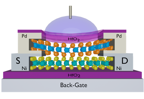
Investigating 2D material heterostructures and ferroelectric gate stacks.
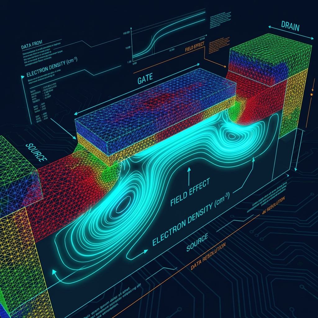
TCAD Simulation & Modelling
Leveraging advanced simulation tools for predictive modelling of next-gen nano-devices.
Selected Publications
Super-Nernstian ion sensitive field-effect transistor exploiting charge screening in WSe2/MoS2 heterostructure
S. Sanjay, M. Hossain, A. Rao, N. Bhat | npj 2D Materials and Applications 5 (1), 93
Precision pH Sensing beyond the Nernst Limit with MoS2/WSe2 Van der Waals Heterostructure Ion Sensitive Field Effect Transistors
A. Tiwari, S. Sanjay, N. B. Mamun, A. Faruq, M. Hossain, N. Bhat | ACS Nano, 2, 2026
Alcohol-Based Sulfur Treatment for Improved Performance and Yield in Local Back-Gated and Channel-Length-Scaled MoS₂ FETs
S. Sanjay, K. Sahoo, N. Bhat | IEEE Transactions on Electron Devices 67 (9), 3711-3715
Super-Nernstian WSe2/MoS2 Heterostructure ISFET Combining Negative Capacitance and Charge Screening Effects
S. Sanjay, F.I. Sakib, M. Hossain, N. Bhat | IEEE Sensors Journal 23 (12), 12526-12535
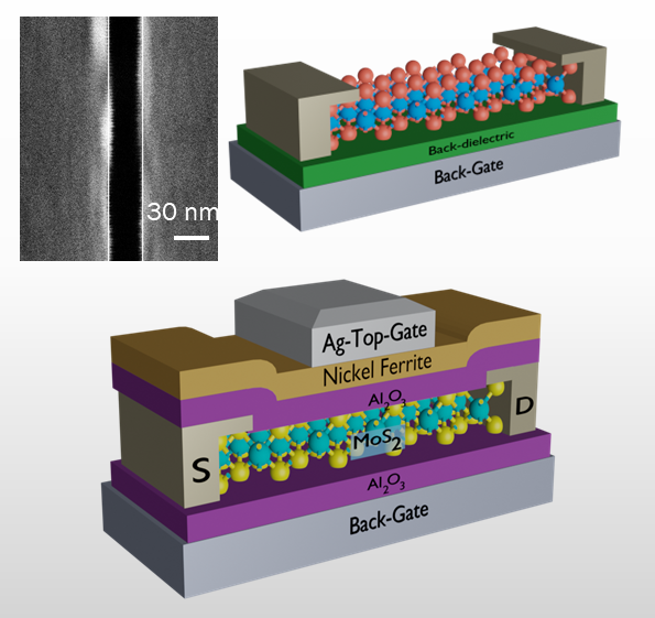
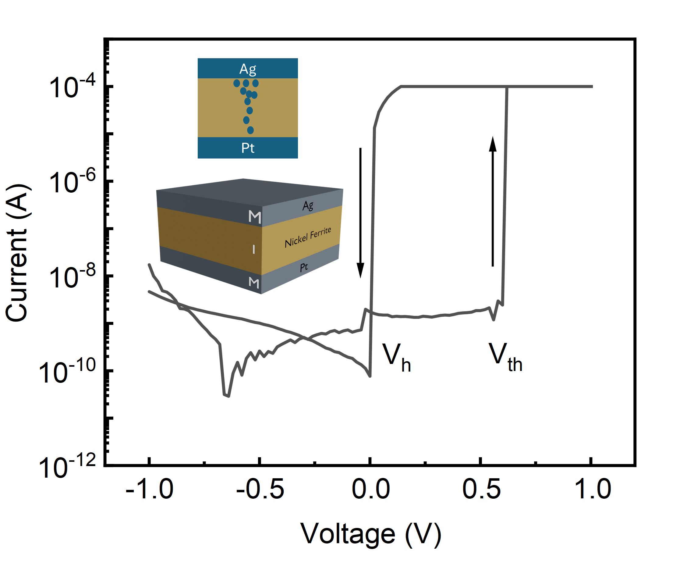
Sub-1 V Threshold Switching in Microwave-Assisted Solvothermal Nickel Ferrite Films and Its Application for Steep Switching MoS2-Phase FETs
S. Sanjay, S. Arackal, A. Paruthi, N. Bhat | ACS Applied Materials & Interfaces 16 (49), 67995-68005
Professional Experience
Postdoctoral Researcher
Tyndall National Institute, University College Cork, Ireland | Aug 2024 – Present Staff Page
View Details
- Investigated band to hopping electronic transport in crystalline oxide semiconductors (WO3, W doped Indium oxide, etc.).
- Conducted low-temperature, and gate-bias dependent Hall measurements in semiconducting oxides.
- Designed the process flow and fabricated electronic test structures on oxide semiconductors, and wire-bonded them.
- Developed process for wire-bonding to ultra-thin semiconductors.
- Collaborated and contributed to experimental workflows within a 9-partner EU consortium project CONCEPT Project
Research Associate
Centre for Nano Science and Engineering, Indian Institute of Science, Bangalore | Feb 2024 – Jul 2024
View Details
- Integrated ferroelectric materials with 2D FETs for low-power logic and memory functionalities.
- Engineered phase-change ferroelectric effect in the gate stack using HfO2 to surpass the Boltzmann limit for enabling steep-switching FETs.
- Used high speed and low temperature electrical measurements to study fluctuations in ferroelectric FETs.
Ph.D. Research Scholar
Centre for Nano Science and Engineering, Indian Institute of Science, Bangalore | Jan 2018 – Mar 2024 Alumni Page
View Details
Thesis: Engineering Nano-Electronic Devices using 2-D Materials: CMOS Logic to Biosensing
- Led end-to-end development of 2D-material FETs — TCAD modeling, design,
fabrication, and characterization — to advance next-generation CMOS logic and
memory technologies.
- Realized 30 nm channel lengths through optimized process & proximity correction in e-beam lithography.
- Developed sub-thermionic MoS2 phase-FET (SSmin = 8.5 mV/dec) by BEOL integration of nickel ferrite with filamentary threshold switching.
- Engineered low resistance, highly reliable, and high yield Ni-MoS2 contacts (RC = 1.3 kΩ μm)
- Optimized functionalization-free top-gate ALD Al2O3 dielectrics on MoS2.
- Defined and fabricated test structures for measuring electrical parameters of 2D materials and their devices.
- Characterized (electrical, material) FETs, ISFETs, and MOSCAPs. Extracted device performance metrics.
- Python-based extraction and statistical analysis of performance metrics from devices.
- Development of 2D-material ISFETs — from TCAD modeling, design, fabrication,
process integration, and characterization — for scalable and CMOS-compatible pH
and biosensing applications.
- Realized super-Nernstian ISFETs surpassing the Nernst limit (SV = 362 mV/pH) based on WSe2/MoS2 heterostructures.
- Developed MoS2 based enzymatic bio-FETs for sensing total-cholesterol.
- Designed, developed, and calibrated physics-based TCAD models for FET and ISFET
device simulations.
- Simulated experimentally calibrated WSe2/MoS2 heterostructures ISFET in TCAD.
- Numerically modeled ferroelectric negative capacitance and combined them with TCAD simulations to demonstrate NC-FETs for steep-switching logic and NC-ISFETs for highly sensitive sensors.
- Mentored 1 Ph.D. student and 1 undergraduate summer intern.
Engineer (Design for Test)
Qualcomm India | Jul 2016 – Dec 2017
View Details
- Point of contact for SoC-level automatic test pattern generation (ATPG) activities for stuck-at and IDDQ faults testing.
- Performed scan-extraction, design rule checking (DRC), and achieved coverage targets (99.25%).
- Generated ATPG test patterns and supported post-silicon validation.
- I was promoted to Engineer after 1 year of experience.
Trainee
Mentor Graphics | Jun 2015 – Jul 2015
View Details
- Studied and developed fully layered test benches for functional verification of designs and systems using System Verilog.
Education
Ph.D., Nano Science and Engineering (Electrical/Electronics Engineering)
Indian Institute of Science, Bangalore | 2018 – 2024
M.Tech. (Research), Nano Science and Engineering (Electrical/Electronics Engineering)
Indian Institute of Science, Bangalore | 2018 – 2024
B.Tech., Electronics and Communication Engineering
National Institute of Technology Calicut | 2012 – 2016
Key Skills
Get In Touch
Feel free to reach out for collaborations or inquiries:
sooraj(dot)sanjay(at)hotmail(dot)com